Pi Pico Controller
This page is the shared reference point for the organiser-built Pi Pico controller, its pinout, and the first pass of nRF24L01+ bring-up. The source hardware files live in the public hack-a-bot-controller repository.
Official References
- Hack-A-Bot controller hardware repository
- Raspberry Pi Pico board documentation
- Raspberry Pi Pico datasheet PDF
- Raspberry Pi Pico SDK hardware API reference
- Nordic nRF24L01+ product specification PDF
What This Page Covers
- the current controller hardware layout
- the real Pico pin map from the KiCad schematic
nRF24L01+pin numbers and wiring on this board- power, test point, and input details that matter during bring-up
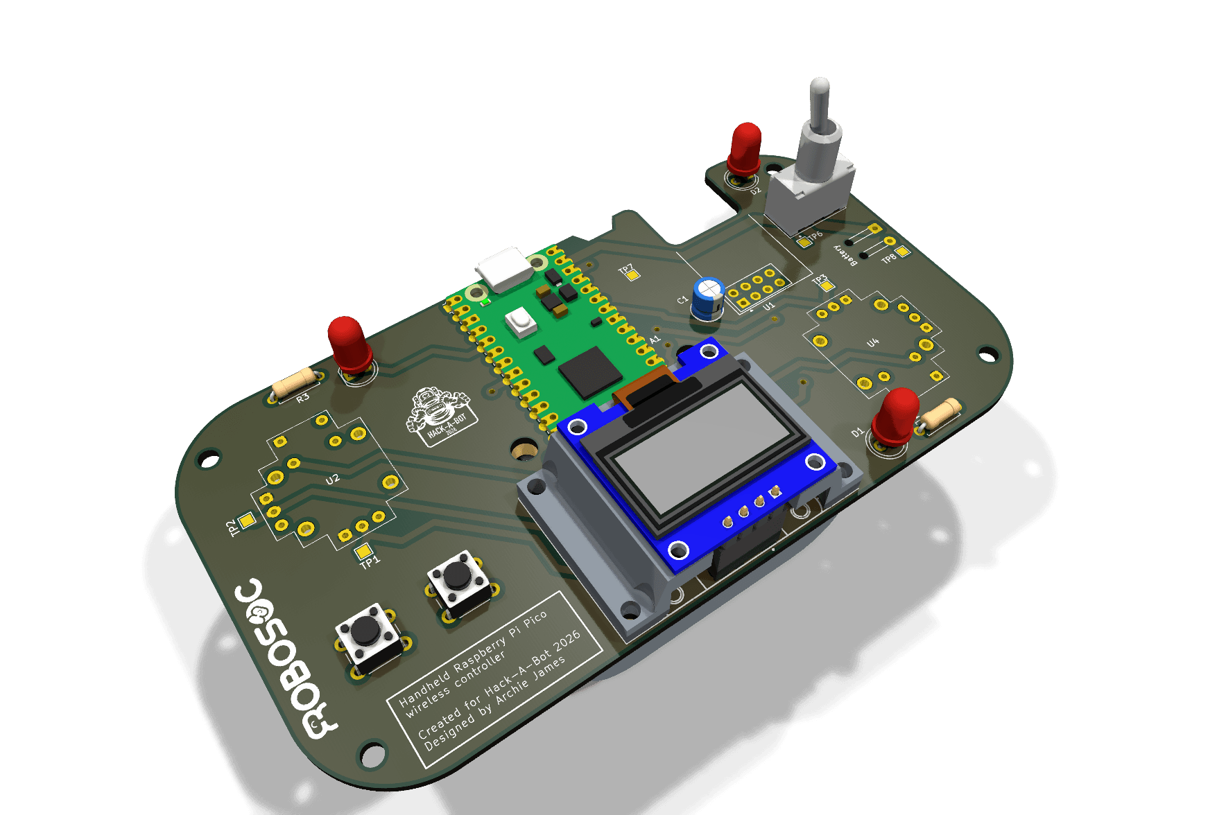
Controller Hardware

Board Summary
From the controller schematic and board files:
- power is designed around a
3xAAbattery pack intoVSYS, with the toggle switch in the battery path - the Pico
3V3rail powers the radio, OLED, joysticks, and buttons - there are
3joystick axes on this revision:Left_H,Left_V, andRight_H - the right joystick vertical axis is not routed on this board revision
- the radio uses Pico
SPI0signals onGPIO4,GPIO6, andGPIO7, withCSNandCEon separate GPIOs - the OLED is wired over I2C on
GPIO20andGPIO21 - battery voltage can be estimated in firmware using the Pico’s internal
ADC3VSYS/3path - the
nRF24L01+IRQpin is not routed to the Pico on this revision
Controller Pinout
These are the current signal assignments from the KiCad netlist:
| Pico Pad | Pico Function | Controller Signal | What It Does |
|---|---|---|---|
5 |
GPIO3 |
STATUS |
status LED drive |
6 |
GPIO4 |
NRF_MISO |
radio SPI MISO |
9 |
GPIO6 |
NRF_SCK |
radio SPI clock |
10 |
GPIO7 |
NRF_MOSI |
radio SPI MOSI |
14 |
GPIO10 |
SW2 |
push button input |
15 |
GPIO11 |
SW1 |
push button input |
16 |
GPIO12 |
Left_SW |
left joystick select button |
19 |
GPIO14 |
NRF_CS |
radio chip select |
22 |
GPIO17 |
NRF_CE |
radio chip enable |
24 |
GPIO18 |
Right_SW |
right joystick select button |
26 |
GPIO20 |
OLED_SDA |
OLED I2C data |
27 |
GPIO21 |
OLED_SCL |
OLED I2C clock |
31 |
GPIO26_ADC0 |
Left_H |
left joystick horizontal axis |
32 |
GPIO27_ADC1 |
Left_V |
left joystick vertical axis |
34 |
GPIO28_ADC2 |
Right_H |
right joystick horizontal axis |
36 |
3V3 |
+3V3 |
logic and peripheral supply rail |
39 |
VSYS |
VBAT |
switched 3xAA battery input |
Unused or not-routed highlights on this revision:
GPIO0,GPIO1,GPIO2,GPIO5,GPIO8,GPIO9,GPIO13,GPIO15,GPIO16,GPIO19, andGPIO22are not assigned to controller featuresGPIO28_ADC2is the only routed axis on the right joystick- the Pico
RUN,VBUS,ADC_VREF, andAGNDpins are not used for controller features - the radio
IRQoutput is left unconnected
nRF24L01+ Bring-up
The official Nordic specification is useful for first principles:
- supply range:
1.9Vto3.6V - host interface:
4-wire SPI - maximum SPI clock:
10Mbps - air data rates:
250kbps,1Mbps, and2Mbps IRQis active low
On this controller, the radio mapping is:
| Radio Pin | Module Signal | Pico Connection | Note |
|---|---|---|---|
1 |
GND |
Pico GND |
common ground |
2 |
VCC |
Pico 3V3 pad 36 |
3.3V only |
3 |
CE |
GPIO17 on pad 22 |
RX/TX enable |
4 |
CSN |
GPIO14 on pad 19 |
SPI chip select |
5 |
SCK |
GPIO6 on pad 9 |
SPI0 clock |
6 |
MOSI |
GPIO7 on pad 10 |
SPI0 TX |
7 |
MISO |
GPIO4 on pad 6 |
SPI0 RX |
8 |
IRQ |
not connected | optional in software, unused here |
GPIO4, GPIO6, and GPIO7 line up with SPI0 receive, clock, and transmit functions, so use spi0 in firmware and drive CSN and CE as ordinary GPIO pins.
Radio Pin Roles
| Pin | What It Does |
|---|---|
VCC |
3.3V radio supply |
GND |
common ground |
CE |
chip enable, used to activate RX or TX mode |
CSN |
SPI chip select |
SCK |
SPI clock |
MOSI |
SPI data from Pico to radio |
MISO |
SPI data from radio to Pico |
IRQ |
interrupt output, active low |
When you wire the radio:
- keep the radio on a stable
3.3Vsupply - make sure the controller and Pico share a common ground
- keep wiring short and tidy
- remember this board has a fitted
10uFdecoupling capacitor at the radio rail and an additional100nFfootprint reserved alongside it - test one clean transmit or receive example before you add extra features
Buttons, Joysticks, and OLED
SW1is onGPIO11andSW2is onGPIO10Left_SWis onGPIO12andRight_SWis onGPIO18- because the push buttons and joystick select lines are tied up to
3V3when pressed, configure those GPIOs with pull-downs in firmware so they do not float when idle - the OLED uses
GPIO20forSDAandGPIO21forSCL - the routed analog joystick channels are
GPIO26_ADC0,GPIO27_ADC1, andGPIO28_ADC2
Test Points
The controller also brings a few useful nets out to labelled test pads:
| Test Point | Signal |
|---|---|
TP1 |
Left_H |
TP2 |
Left_V |
TP3 |
Right_H |
TP4 |
OLED_SDA |
TP5 |
OLED_SCL |
TP6 |
VBAT |
TP7 |
+3V3 |
TP8 |
GND |
Bring-up Checklist
- Confirm the Pico builds and flashes from VS Code.
- Configure pull-downs on
SW1,SW2,Left_SW, andRight_SW, then confirm the digital inputs switch cleanly. - Read
Left_H,Left_V, andRight_HonADC0,ADC1, andADC2, and add a calibration deadzone before you trust the joysticks. - Confirm the OLED comes up on
GPIO20andGPIO21, usually at I2C address0x3C. - Bring up the radio on
spi0withMISO=GPIO4,SCK=GPIO6,MOSI=GPIO7,CSN=GPIO14, andCE=GPIO17. - Prove a simple send or receive test before you start controlling motors or mechanisms.
- If you need battery telemetry, read the Pico’s internal
ADC3VSYS/3path and calibrate it against a meter.
Common Failure Points
- unstable
3.3Vpower to the radio - mixed-up chip-select or IRQ wiring
- forgetting common ground between modules
- forgetting to enable pull-downs on the button inputs, which leaves them floating
- assuming the right joystick has two analog axes on this revision when only
Right_His routed - trying to debug radio, OLED, and input logic all at the same time
More Help
If the controller-specific mapping is still unclear after checking the schematic and repo, ask a supervisor.